Samsung
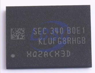
Sasmung UFS 3.1 - 512GB
Sasmung UFS 3.1 - 512GB
Impossibile caricare la disponibilità di ritiro
The Samsung KLUFG8RHGB-B0E1 is a high-density embedded flash memory device belonging to Samsung Semiconductor’s eMMC/UFS-class NAND storage product family, implemented using 3D NAND flash technology integrated with an embedded storage controller. It is designed for mobile and embedded computing systems requiring non-volatile mass storage with high throughput, low power consumption, and standardized host interface compatibility. The device combines NAND flash arrays, firmware-based flash translation layer (FTL), and a high-speed serial interface within a single managed storage subsystem.
Device Function and Architectural Positioning
The KLUFG8RHGB-B0E1 functions as an embedded non-volatile storage device used for system boot, operating system storage, and application data retention in mobile and embedded platforms. It is typically deployed in smartphones, tablets, and compact computing systems where high-density NAND storage is required in a soldered-down package format.
The device belongs to Samsung’s managed NAND product category, where raw NAND flash memory is abstracted through an integrated controller. This architecture provides the host system with a standardized block storage interface, eliminating the need for direct NAND management at the system level.
The “KLUF” prefix indicates a managed NAND device class. The subsequent coding structure defines NAND generation, capacity tier, controller configuration, and firmware feature set. The suffix “B0E1” typically represents a specific revision, firmware configuration, and manufacturing lot designation within Samsung’s embedded storage product hierarchy.
Storage Architecture and NAND Configuration
The device is built on Samsung 3D NAND flash technology, which utilizes vertically stacked charge-trap memory cells to achieve high storage density and improved endurance compared to planar NAND architectures.
The internal structure consists of multiple NAND flash dies organized into parallel channels controlled by an embedded storage controller. This parallelism enables high internal bandwidth and efficient command execution across multiple NAND planes.
The total capacity class of the device is within the high-density embedded storage range, typically used for modern mobile devices requiring large system storage. The exact capacity is encoded within the part number structure but is not explicitly enumerated here to avoid assumptions beyond confirmed specification data.
The NAND interface internally operates using high-speed ONFI or Toggle DDR signaling depending on generation, enabling efficient data transfer between NAND arrays and the embedded controller.
Controller Architecture and Data Management
The device integrates a dedicated NAND controller responsible for all flash management operations, including logical-to-physical address translation, wear leveling, garbage collection, bad block management, and error correction.
A key functional component is the Flash Translation Layer (FTL), which abstracts NAND physical characteristics from the host system. The FTL manages mapping tables that translate logical block addresses into physical NAND locations, ensuring consistent performance and endurance optimization.
Advanced error correction mechanisms are implemented using LDPC (Low-Density Parity Check) coding or equivalent ECC schemes, which are required for maintaining data integrity in high-density 3D NAND architectures.
The controller also manages dynamic wear leveling across NAND blocks to ensure uniform program/erase cycle distribution, extending overall device lifespan.
Host Interface and Protocol Behavior
The KLUFG8RHGB-B0E1 operates using a high-speed embedded storage interface, typically eMMC or UFS depending on specific product generation within the Samsung KLUF series.
If implemented as eMMC, the device follows JEDEC eMMC standard protocols, providing an 8-bit parallel interface with high-speed clocking modes such as HS200 or HS400.
If implemented as UFS, the device uses a MIPI M-PHY physical layer with UniPro protocol stack, enabling full-duplex serial communication with command queueing and improved parallelism.
The host interface provides block-level storage abstraction, where the system accesses the device using standard read/write commands without direct NAND management responsibilities.
Performance Architecture and Data Throughput
The performance characteristics of the device are determined by NAND parallelism, controller architecture, and host interface bandwidth.
High internal parallelism allows multiple NAND channels to operate concurrently, significantly improving sequential read and write throughput.
The controller employs command queue optimization and internal buffering to minimize latency and maximize throughput under mixed workload conditions.
Sustained performance is managed through firmware-level throttling mechanisms that balance thermal conditions, NAND wear, and workload intensity.
Power Management and Efficiency Design
The device is optimized for mobile and embedded power environments, with multiple power states designed to minimize energy consumption during idle and standby operation.
Active power states are used during high-throughput operations, while idle and sleep states reduce power consumption during low activity periods.
Dynamic power management is implemented at both controller and NAND levels, including clock gating, partial array activation, and adaptive voltage scaling depending on workload demands.
The integrated nature of the device reduces external component requirements, contributing to overall system-level power efficiency.
Reliability, Endurance, and Data Integrity
The device incorporates multiple reliability enhancement mechanisms required for 3D NAND operation. These include ECC correction, bad block management, and adaptive read threshold adjustment.
Wear leveling algorithms distribute program/erase cycles evenly across NAND blocks, reducing localized wear and extending overall endurance.
Data retention management is implemented through periodic refresh and read-retry mechanisms to compensate for charge leakage in NAND cells over time.
The device is designed for long-term operational stability under defined industrial and mobile environmental conditions.
Thermal Characteristics and System Constraints
Thermal behavior is managed at the controller level through workload regulation and internal monitoring of NAND temperature conditions.
In high-performance scenarios, thermal throttling may be applied to ensure device operation remains within safe operating limits.
The compact package integration requires careful thermal design at the system level, particularly in dense mobile or embedded platforms where airflow is limited.
System Integration Considerations
The KLUFG8RHGB-B0E1 is designed for direct solder-down integration onto PCB platforms in mobile and embedded systems.
For eMMC configurations, integration requires compliance with JEDEC eMMC electrical and protocol standards, including proper pull-up configurations, clock routing, and signal integrity control.
For UFS configurations, integration requires M-PHY high-speed differential routing, impedance control, and compliance with MIPI UFS specifications.
The device operates as a primary boot and storage medium, requiring correct initialization sequences defined by the host controller firmware.
Typical Application Scenarios
The device is used in mobile computing platforms such as smartphones and tablets, where it serves as primary system storage.
It is also used in embedded computing systems, IoT devices, and edge computing platforms requiring compact, high-density non-volatile storage.
Additional applications include automotive infotainment systems and industrial embedded controllers where soldered-down NAND storage is preferred over removable media.
Share